OTA模拟代写 模拟电子电路代写 EE4312代写 ee电子电路代写
598EE4312 Design Project Intermediate Assignment: OTA simulation + Specifications OTA模拟代写 For your project progress meeting with the TAs in the week of Nov. 29 2021, you are asked to pr...
View detailsSearch the whole station
模拟电子电路代写 Project Description You need to design an on-chip CMOS feedback amplifier that can drive an oscilloscope input. The input impedance of
You need to design an on-chip CMOS feedback amplifier that can drive an oscilloscope input. The input impedance of your oscilloscope is 1MOhm in parallel with 20pF; please review the statement from Prof. Lee on pp.111-112 in this reference1 about oscilloscope inputs and probes.
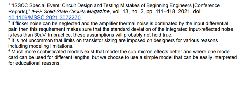
The use of your amplifier is to buffer with a gain of G on-chip signals when they are routed to the outside to be measured with an oscilloscope. Your amplifier needs to have a high input impedance and needs to enable an accurate measurement of DC voltages on chip with an accuracy of 0.1%. Additionally, within the given power budget you want to achieve as fast a step response as possible with an overshoot of less than 1%. You further want to support as large an input and output signal range as reasonably possible. You also need to keep the noise of the amplifier sufficiently low; we incorporate this into the design specifications by requiring2 that
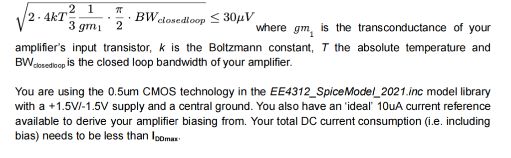
all transistors in your design need to have a Vov of at least 200mV. You can use any W >= 1um and L = 0.5um, 1um, 2um, 4um or 8um with the associated model cards given below. The models provided are LEVEL 2 models4 which are simple models, however, they have the benefit that parameters and the .OP results can easily be interpreted. In order to obtain proper output conductances, a different model card is provided for different transistor lengths. You can assume that LDIF = 2*LMIN or 1um. For a simple transistor layout AD = AS = W*LDIF and PS = PD = 2W + 2LDIF and you can adjust these if you recommend to
use fingered transistor layouts.
| L | Model Card NMOS | Model Card PMOS |
| 0.5um | CMOSN_05 | CMOSP_05 |
| 1um | CMOSN_1 | CMOSP_1 |
| 2um | CMOSN_2 | CMOSP_2 |
| 4um | CMOSN_4 | CMOSP_4 |
| 8um | CMOSN_8 | CMOSP_8 |
Determine a block diagram for your amplifier; we strongly recommend to start with a two-stage operational transconductance amplifier (OTA) in a non-inverting feedback topology.
Try to determine the necessary DC gain, gain-bandwidth, phase margin, … to meet the specifications of the amplifier outlined above. Try to verify using simulations of a model of your amplifier.
Note: Design always requires working through a puzzle of interdependent requirements and you might not immediately understand how to go from the feedback amplifier specifications to the OTA specifications. Then just make some assumptions, proceed and later, once you understand the interdependencies better, go back and revisit your assumptions.
Size the components in your amplifier to meet your requirements and verify with simulations if they do. Make sure to verify the proper biasing of the amplifier with a .OP simulation, run .AC simulations to check open and closed-loop gain, run a .DC simulation to obtain the input/output characteristic and run transient simulations (.TRAN) for the step responses. Pay attention to making a well organized simulation test bench. 模拟电子电路代写
Fine tune your component sizing and resimulate so that you meet the requirements and optimize the performance. The main goal is to deliver an amplifier that properly works; so better to have a slower amplifier that works than a potentially fast amplifier that does not work. If you have time, but this is not required, you can consider topology improvements.
Run extensive simulation to characterize the design and make a performance table at room temperature (27degC); report on the operating point, frequency responses and stability, DC transfer function, and step responses for a set of five step amplitudes between 10mV to your max. input voltage, both positive and negative.
Run process-voltage-temperature verification; you only need to run the simulation and observe the performance changes; you do not need to redesign the amplifier to meet the requirements across PVT for this project.
a. Voltage variation:
i. Temp = 27degC and 0.9 VDD, VDD, 1.1 VDD
b. Temperature variation:
i. VDD and 0degC, 27degC, 80degC
c. Process variation:
i. skip
d. Load variation:
i. What happens when your amplifier is not directly connected to the scope but is connected through a 10x probe.
You need to submit a report on your design. The report is limited to 20 pages and needs to be submitted as a PDF in courseworks. Grading will be based in part on the performance of the design, but in a larger part on you demonstrating that you understand your design in and out.
The report should be written for peer designers so they understand the design choices and optimizations you made and how and why.
○ That means that you do not have to explain basic design concepts and no need to copy anything from books or the lecture notes, but rather explain and motivate your reasoning and design approach. E.g., how did you choose bias currents, Vov, W/L, L of your devices.
○ Make sure to demonstrate that you can explain the operation of your design in detail. E.g., confirm the AC simulation results with hand calculations based on your understanding of the operation of your amplifier.
○ Similarly for other performance metrics. E.g., does the time domain behavior (step response) correspond to what you expect from the frequency domain characteristics for all step amplitudes. Can you explain the input and output signal ranges.
○ When there are discrepancies between simulations and calculations try to identify their causes. 模拟电子电路代写
The report needs to include all relevant schematics. It is OK to cut and paste schematics from LTspice, but choose an appropriate background color and zoom level. There is no need to redraw your schematics in a drawing tool, just make sure things are readable. Important: make sure to name your devices and nodes in your schematics so plots and netlists can be easily understood.
The report needs to include a spice netlist of your design.
The report needs to include an operating point simulation print out of your design as well as a table summarizing the operating points of the key transistors and their key small signal parameters.
The report needs to include the necessary summary tables reporting on the performance of your design. You can think of this part as a mini datasheet.
The report needs to include plots of the relevant simulation waveforms; make sure to annotate (even by hand if you like) the plots to indicate key performance metrics that you extracted from the simulation.Working in groups:
You can work in groups of two. Fill out your name in this sign up sheet
Each group only needs to submit one report.
Make sure to clearly mark your names on the report.
On the front page also state the relative contribution of each group member.

更多代写:CS圣路易斯华盛顿大学代写 toefl在家考 英国数学Midterm代考 article统计学作业代写 外国大学毕业论文代写 国外Python代考

EE4312 Design Project Intermediate Assignment: OTA simulation + Specifications OTA模拟代写 For your project progress meeting with the TAs in the week of Nov. 29 2021, you are asked to pr...
View details
I218 Computer ArchitectureReport 3 计算机体系结构cs代写 (1) In the textbook and lecture slides, detailed information in the pipeline registers (IF/ID, ID/EX, EX/MEM, MEM/WB) is not provided. ...
View details
I218 Computer ArchitectureReport 2 cs计算机体系结构作业代做 (1)How is the instruction “sub $t9, $s4, $s7” translated to a machine instruction code? Answer the rs, rt, and rd fields in binary n...
View details
Economics 426: Problem Set 1 – Robinson Crusoe 经济问题集代做 I. Robin Crusoe is endowed with 112 labor-hours per week. There is a production function for the output of oysters Spring...
View details