电力系统分析代写 Power Systems Analysis代写 EE代写
1021QUIZ 1 EEE406 Power Systems Analysis 电力系统分析代写 INSTRUCTIONS TO CANDIDATES 1. This paper consists of 2 questions. Answer ALL questions. 2. Read the above information carefully to ...
View detailsSearch the whole station
电子电路设计代写 Instructions: 1.This exam is close book, close notes. You may use a calculator but it may not be shared with anyone else during the exam.
[5×3 pts=15 pts]
(a) Multiple choice questions :
(i) In the current mirror shown below, if (W/L)Q2 : (W/L)Q1 = 2:1 and (W/L)Q4 : (W/L)Q3 = 1:2 then I0 is:
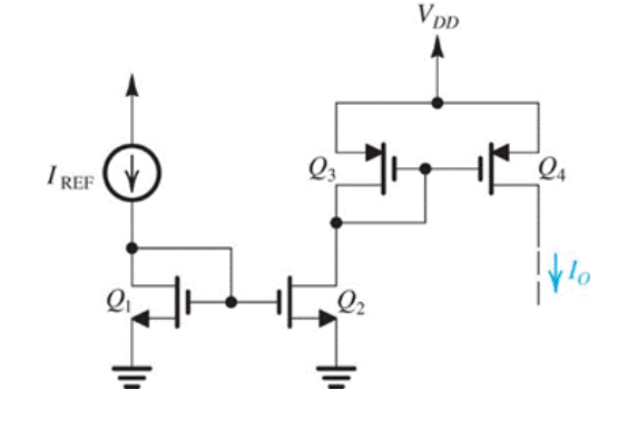
(a) I0= Iref
(b) I0 = 2Iref
(c) I0 = 4Iref
(d) I0 = 0.5Iref
(iii) In the following differential amplifier, if VCM=1V then source potential VS is
(a) 0V
(b) -1.5V
(c) -1.0V
(d) -2.0V
(iv) A BJT transistor operating in active mode has IE = 1mA and IB = 10µA, then β is
(a) 990
(b) 100
(c) 99
(d) 1
(v) In the common source amplifier circuits show below the relationship between overdrive voltages (VOV) of CS-x and CS-y is
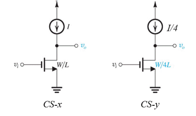
(a) VOV of CS-y is 4 times than VOV of CS-x
(b) VOV of CS-y is 2 times than VOV of CS-x
(c) VOV of CS-y is same as VOV of CS-x
(d) VOV of CS-y is 0.5 times than VOV of CS-x
[5×4=20 pts]
Consider the FET amplifier shown below for the case VDD =1.8V, VGS = 0.6V, k’n(W/L) = 5mA/V2 , Vt = 0.4V and RD = 10kΩ. Note that VDS is DC bias and vgs is small signal voltage.
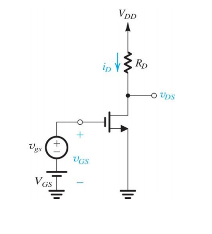
(a) Find the DC quantities ID and VDS.
(b) Calculate the value of gm at the bias point
(c) Calculate the value of voltage gain.
(d) If the MOSFET has λ=0.1V-1 , find ro at the bias point and calculate the voltage gain.
[20 pts]
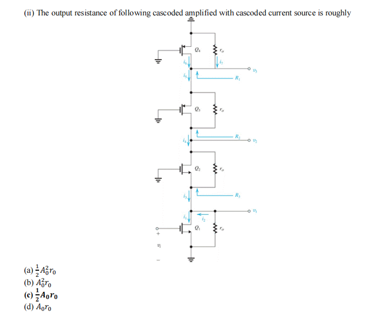
(a) In a MOS cascode amplifier, the cascode transistor is required to raise the output resistance by a factor of 50. If the transistor is operated at VOV =0.2V, what must be its VA be?
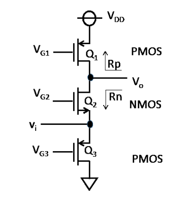
(b) Find the gain of the following amplifier in terms of gm and ro of transistors (gm of Q1 is gm1, ro of Q1 is ro1 and so on). (Hint: Think about output resistance of NMOS “Rn” and input resistance of PMOS “Rp”).
[10+15=25 pts]
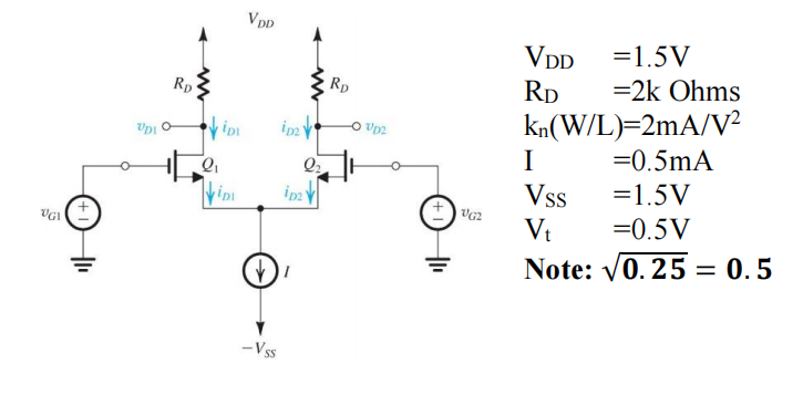
In the circuit below ID =100µA, all transistors have VOV =0.5V and VA = 3.6V. (µnCox = 4µpCox = 100µA/V2 ).
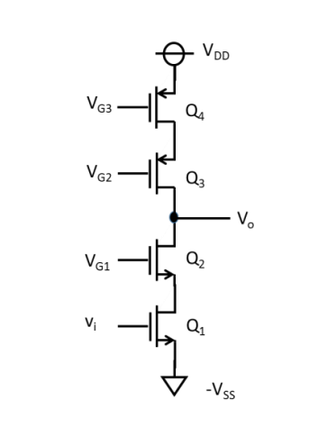
(a) Find (W/L) of all transistors.
(b) Find the gain, input and output resistances.
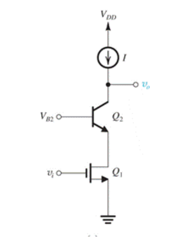
[20 pts]
Given the following data, calculate the Gm, RO and Avo of the amplifier circuit shown below: I =100µA, β=125, W/L=25, VA =1.8V, µnCox = 400µA/V2 .
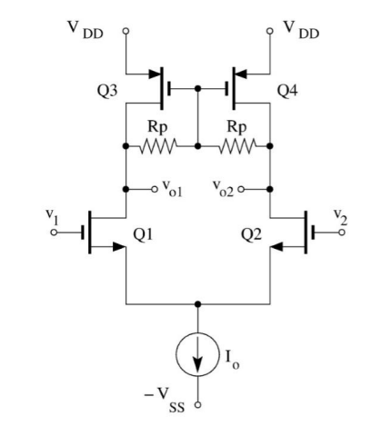
[10 pts]
Assume Q3 and Q4 as well as Q1 and Q2 are identical and their output resistance is r0. Compute the expression for differential gain.
Hints: (i) You can use half-circuit analysis. (ii) DC nodes can be grounded for small signal analysis.

更多代写:R studio代写 多邻国考试作弊 英国bio网课代修价格 英国硕士毕业论文字数 apa引用格式生成器 学术抄袭
合作平台:essay代写 论文代写 写手招聘 英国留学生代写

QUIZ 1 EEE406 Power Systems Analysis 电力系统分析代写 INSTRUCTIONS TO CANDIDATES 1. This paper consists of 2 questions. Answer ALL questions. 2. Read the above information carefully to ...
View details