计算机组件和操作课业代写 ECSE 2610代写 四位加法器代写
ECSE 2610 Computer Components and Operations
Studio 3
Four Bit Adder
计算机组件和操作课业代写 Objective: The objective of this studio is for you to learn how to use structural/modular design in VHDL to create a real world application by
Objective:
The objective of this studio is for you to learn how to use structural/modular design in VHDL to create a real world application by implementing an adder unit on an FPGA chip and display the addition result.
You will use Xilinx Vivado software to implement a 4-bit adder circuit. You will then connect the result of the adder to the input of your display drivers (from the previous studio). Finally, you will download the circuit design to the board and will test proper functionality of the circuit. Eight bit slide switches should be used for implementing two 4-bit numbers as inputs, the addition should be outputted in hexadecimal form on two seven segment displays.
Discussion: 计算机组件和操作课业代写
We will also introduce modular design for VHDL. This is a powerful tool to streamline FPGA design, avoid code repetition and enhance portability, re-usability and abstraction.
For this lab, you will need to write VHDL modules for three components and then instantiate them in the toplevel.vhd file. Look at examples in the modular VHDL tutorial on Piazza under studio resources for syntax and usage.This will save you a lot of time. The tutorial walks you through three main steps involved in writing the toplevel module; component declaration, signal declaration, and component instantiation (port mapping).
Components involved in this design: 计算机组件和操作课业代写
1-bit full adder: bit_full_adder.vhd
You should write a new behavioral VHDL source to add three bits at a time.
Inputs: A, B, Cin.
Outputs: S, Cout.
Include the expressions for sum and carry out of the 1 bit full adder. Use the classic truth table, Kmap, Sum-Of-Products approach to get the equations for your outputs.
display_driver: Display_driver.vhd
You have already done this in a previous studio. This component takes in a 4-bit input and outputs 7 bits controlling the 7 segments. Just download it from Piazza and add it as an existing source to your current project. Will be added to studio resources section after studio 2 due date.
LEDdisplay: LEDdisplay.vhd 计算机组件和操作课业代写
This component is used to switch between the outputs of display_driver1 and display_driver2 on two different 7-segment displays (refer the block diagram attached on Piazza; most useful resource for this studio). This source is also provided for your use. Just download it from Piazza and add it as an existing source to your current project.
Your outputs on the 2 seven segments will range from 00 to 1E.
Putting everything together: Toplevel design toplevel.vhd
Write a new VHDL source that puts all components you have designed or added to your project so far together, and make proper interconnections between these components as per the block diagram given.
Toplevel Entity: The overall inputs and outputs shown in the block diagram are the I/O to the dashed box, i.e. 8 slide switches, carry_in, clock, anodes, segments.
Toplevel Architecture: This can be divided into three steps. 计算机组件和操作课业代写
1.Component Declaration (before begin statement): Each unique component used in your design should be declared here. Component declaration is very similar to writing entity of the module you want to use in your toplevel design.
2.Signal Declaration (before begin statement): Every output in your design that is not the final output needs to be declared as a signal. That is, all intermediate outputs. This is done so that you are able to make proper interconnections during the next step.
3.Component Instantiation or Port Mapping (after begin statement): This is where you make all the interconnections between components. Example of a port mapping statement below:
Arbitrary_Unique_Label: Name_of_component port map ([input/output variable inside the component] => [variable outside the component]);
Refer to more examples in the modular VHDL tutorial.
Design Constraints: .xdc file for toplevel 计算机组件和操作课业代写
You need to create a new XDC file for the toplevel inputs and outputs. You can use any one of the push-buttons or a slide switch as carry_in. Use the onboard clock of 100 MHz as your clk input.
Synthesize, Implement, and Download Bitstream to FPGA board.
Verify that correctness of your design by testing the adder for arbitrary 4-bit inputs. Change inputs using the slide switches and make sure that you get the correct corresponding output in hex form. Check whether or not your result increments by 1 when carry_in is 1. If you get incorrect outputs retrace your steps making sure you have correct pin assignments and that your VHDL is correct. After you’ve tested circuit for proper operation, show it to your TA. Specific test cases are listed on the last page of this document.
Schematic of your design can be viewed by: 计算机组件和操作课业代写
Flow Navigator window on the left of your screen → RTL Analysis → Open elaborated design Demonstrate your work to the TA and get checked off. While check off, the TAs may ask you a couple of questions to check your understanding. After you are done with the studio work, turn off your FPGA board, gently unplug the USB cable from the board and coil it. Place the board in the box with foam padding and keep both the box and cable in a safe place away from food or drinks.
Studio 3 write-up should be uploaded to Gradescope. It should include the following deliverables:
1.(5 pts) Boolean expressions for sum and carry out outputs of full adder component.
2.(10 pts) VHDL code for one bit full adder and toplevel.
3.(5 pts) XDC file.
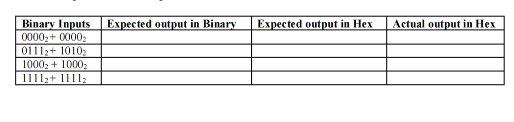
4.(5 pts) For this particular studio, the student should demonstrate the correct working of their design for the following 4 cases.
Due on Gradescope March 10th at 11:59 pm eastern. One submission per team of 2 students. Add your team member to the submission after uploading work. Partners should check if they were added to the submissions.

更多代写:C/C++作业代写 托福家庭版保分 英国Chemistry化学代上 Cause and Effect Essay代写 Australia英语论文 web代写机构
合作平台:essay代写 论文代写 写手招聘 英国留学生代写